
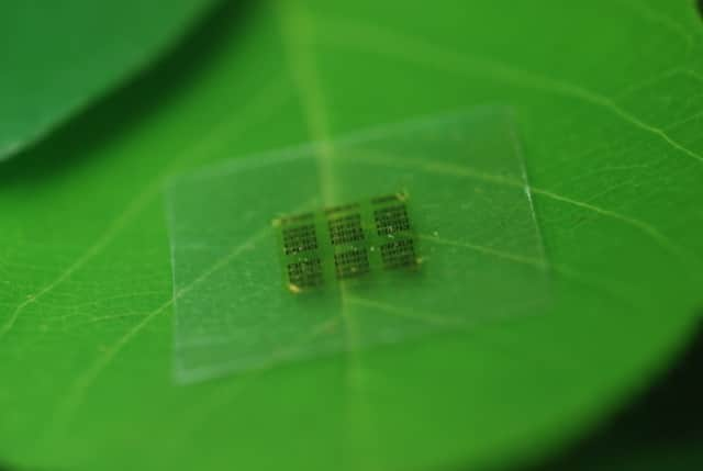
 computer chip rests on a leaf. Photo- Yei Hwan Jung, Wisconsin Nano Engineering Device Laboratory")
In an effort to alleviate the environmental burden of electronic devices, a team of University of Wisconsin-Madison researchers has collaborated with researchers in the Madison-based U.S. Department of Agriculture Forest Products Laboratory (FPL) to develop a surprising solution: a semiconductor chip made almost entirely of wood.
Developed by researchers at the University of Wisconsin-Madison and the U.S. Department of Agriculture Forest Products Laboratory and detailed in a research paper published this week in Nature Communications, “Wood chips” takes on new meaning with a new green technology, cellulose nanofibril (CNF). The “chips” in question are indeed made mostly of wood but they are also computer chips. As of 2007, eight years ago, about 3.2 million tons of electronic waste was being generated each year, the researchers noted. The paper shows the feasibility of replacing the substrate of a computer chip, with cellulose nanofibril (CNF), a flexible, biodegradable material made from wood.
The research team, led by UW-Madison electrical and computer engineering professor Zhenqiang “Jack” Ma, described the new device. “The majority of material in a chip is support. We only use less than a couple of micrometers for everything else,” Ma says. “Now the chips are so safe you can put them in the forest and fungus will degrade it. They become as safe as fertilizer.”
Zhiyong Cai, project leader for an engineering composite science research group at FPL, has been developing sustainable nanomaterials since 2009. “If you take a big tree and cut it down to the individual fiber, the most common product is paper. The dimension of the fiber is in the micron stage,” Cai says. “But what if we could break it down further to the nano scale? At that scale you can make this material, very strong and transparent CNF paper.”
Yei Hwan Jung, a graduate student in electrical and computer engineering and a co-author of the paper, says the new process greatly reduces the use of such expensive and potentially toxic material. “I’ve made 1,500 gallium arsenide transistors in a 5-by-6 millimeter chip. Typically for a microwave chip that size, there are only eight to 40 transistors. The rest of the area is just wasted,” he says. “We take our design and put it on CNF using deterministic assembly technique, then we can put it wherever we want and make a completely functional circuit with performance comparable to existing chips.”